This blog will help you find all the essential articles needed for a beginner in the field of Physical Design.This blog will be a collection of my ideas,thoughts and resources based on my experience in technology.Topics that will be covered here includes VLSI Physical Design flow, Static Timing Analysis(STA), Low Power concepts etc.I wish to include more topics in the future.
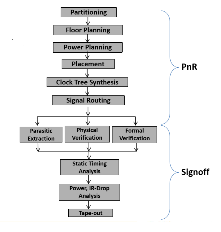
The process of converting a gate-level netlist (written using your Hardware Description Language(HDL)) into GDSII (Geometric Datastream) or physically realizable format(having geometric shapes) which finally becomes a hardware is called Physical Design.
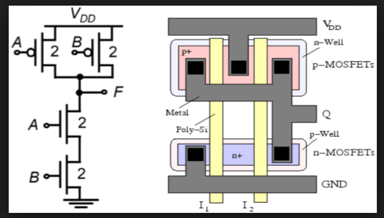
fig: simple transistor level circuit converted into a physically realizable format
Structural representation to physical implementation (ie.,) Netlist to GDS.
->Technically, they are complex designs with multiple embedded processors, memory subsystems, and application specific peripherals on a single piece of Silicon.
->In today’s world everyone wants a handy computer I mean something very compact that can perform all functions of a laptop/PC on a small device. We all carry Tablets or smartphones these days, which can perform all the functions of a PC., like gaming, media streaming, application specific tasks etc.
-> If you look into the motherboard architecture of a computer it will have all the peripherals and components required for proper functioning and since its a huge chip with several components one can see the heat sinks and cooling fans present to reduce the heat generated since these processors are power hungry. This defines what we call a System on Chip(SOC).
-> All the components seen on a motherboard are all integrated on a single compact chip in smartphones/tablets. The SOC size is as small as a coin.
->Architecture of processor used in PC/laptop is different from that used in smartphone. Mobile processor uses ARM architecture, because SOC’s that uses this architecture are more powerful and power efficient. Operating systems(OS) in the smartphones is optimized for this SOC’s. Its because of this software optimization smartphones are able to outperform the PC’s these days.
->Large number of Intellectual Properties(IP’s) are used for an SOC design.
IP core is a block with logic or data that is used in making Application Specific Integrated Circuits (ASIC) or Field Programmable Gate Array (FPGA) for customers/products.
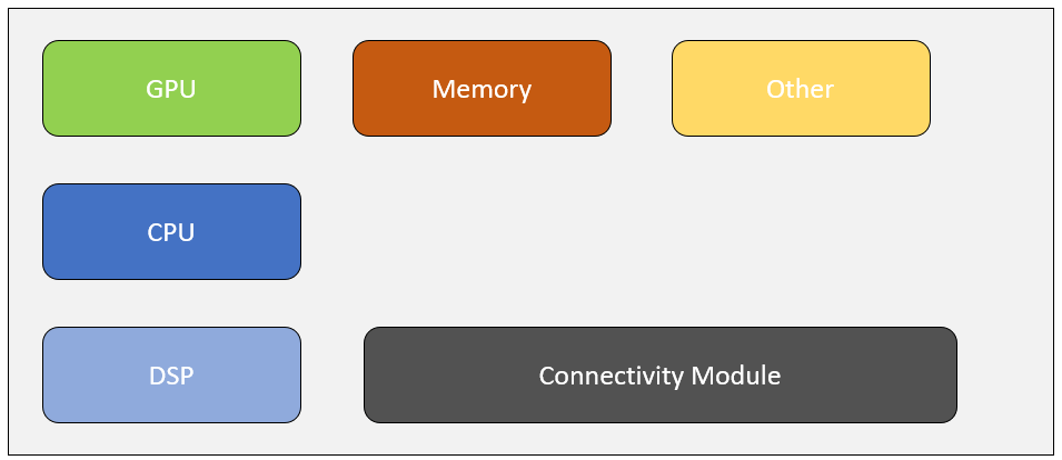
Inside a SOC:
CPU-Processor (Main important component of a SOC)
GPU-Responsible for all the graphics related activity on your device.
DSP- Audio processing, video processing,Display
Memory: RAM(volatile memory) , ROM (Storage memory).
Other modules: Camera, Location, security, sensors.
Due to size constraints, sometimes we can’t accommodate the memory inside the chip. Inside the chip/On-chip (SRAM), Outside the chip/Off-chip(DRAM). In such cases memory package is stacked above this which reduces cost and size(Package On Package[PoP]).
In that case we need to establish connection between CPU and memory.This is done using module called North Bridge.
I am Yamini Parthasarathy. I have strong passion towards Digital VLSI concentrating on Physical Design (P&R,STA,Low power techniques and concepts), VLSI(CMOS concepts).I did my Physical Design training with Gigascale Design System (Bengaluru,India) for 4-5 months post which I joined as a Physical Design Intern at Cadence Design System,Bengaluru. I worked as a Physical Design Engineer for close to 2 years.
I moved to USA for my Masters in Electrical Engineering (Major: Computing systems) at University of Texas at Dallas. I interned with Qualcomm Inc during my Summer 2018. I have worked on different technology nodes (7nm, 16nm,28nm, 130nm,180nm). I have good knowledge on the Industry’s latest tools and scripting languages. I would like to share my knowledge through this blog.
The main motive of this blog is to create awareness within students for VLSI/Semiconductor industry.